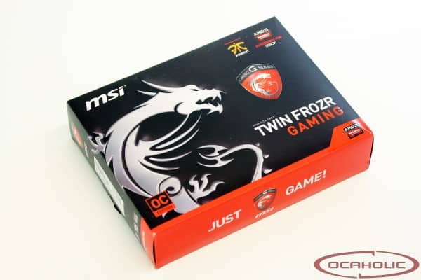
 In the past few days we’ve published no less than three MSI Gaming Series graphics card reviews. Today we’re having a closer look at MSI’s R9 280X Gaming OC Edition graphics card and what it has to offer in details. A quick look reveals, there is a Twin Frozr IV cooler mounted on a reference PCB, which sounds like a combination that offers a very solid price/performance ratio.
These days we are re having quite a good run reviewing a few MSI Gaming Series graphics cards. Today, we have a chance to check out the R9 280X which features a Twin Frozr IV custom cooler but with a reference PCB. With its black and red color scheme this card looks just about perfect on any MSI Gaming Series motherboard and luckily the manufacturer also decided to slightly overclock the GPU.
Since this is a Twin Frozr Gaming version of the MSI Radeon R9 280X series, the graphics card features a slight factory overclock of 50 MHz for the core. While a standard reference Radeon R9 280X GPU is set to work at 850 MHz for the base GPU clock and 1’000 MHz for the Boost GPU clock, the MSI Twin Frozr Gaming R9 280X OC Edition works at 1000 MHz for the base clock and 1’050 MHz for the Boost GPU clock.
Unfortunately, no factory overclocking was done on the 3GB of GDDR5 memory which remains at the recommended 1’500 MHz (6’000 MHz effective).
During our testing the MSI Twin Frozr Gaming R9 280X OC Edition held 1’050 MHz most of the load time. We have only experienced downclocking under FurMark where the GPU clock was going up and down from 1’020 MHz to 1’000 MHz. We did not notice any throttling while gaming.

| MSI Twin Frozr Gaming R9 280X OC Edition | R9 280X TurboDuo OC | R9 280X DC II Top | Radeon R9 280X | |
| Chip | Tahiti XT2/L | Tahiti XT2/L | Tahiti XT2/L | Tahiti XT2/L |
| Process | 28 nm | 28 nm | 28 nm | 28 nm |
| Transistors | 4.31 billion | 4.31 billion | 4.31 billion | 4.31 billion |
| GPU clock | 1’000 MHz | 880 MHz | 1’070 MHz | 850 MHz |
| GPU Boost clock | 1’050 MHz | 1’030 MHz | N/A | 1’000 MHz |
| Memory GDDR5 | 3’072 MB | 3’072 MB | 3’072 MB | 3’072 MB |
| Memory clock | 1’500 (6’000) MHz | 1’500 (6’000) MHz | 1’600 (6’400) MHz | 1’500 (6’000) MHz |
| Memory interface | 384 Bit | 384 Bit | 384 Bit | 384 Bit |
| Memory bandwidth | 288.0 GB/s | 288.0 GB/s | 307.2 GB/s | 288 GB/s |
| Shader Cores | 2’048 | 2’048 | 2’048 | 2’048 |
| TMUs | 128 | 128 | 128 | 128 |
| ROPs | 32 | 32 | 32 | 32 |
| PCB Type | Custom Design | Reference Design | Custom Design | Reference Design |
| Lenght (PCB – Total) | 26.8 | 26.8 cm | 28.7 cm | xx.x – xx.x cm |
| Height (PCB – Total) | 11.8 cm | 13.0 cm | 14.8 cm | xx.x – xx.x cm |
| Slots | 2 | 2 | 2 | 2 |
| Cooler | Twin Frozr IV | TurboDuo | DirectCU II | AMD Reference |