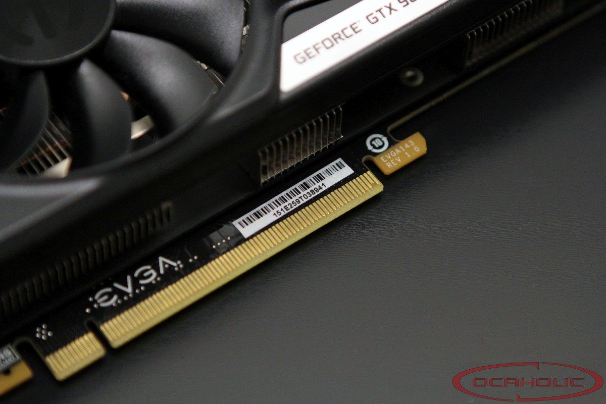
With the GTX 960 SSC ACX 2.0, EVGA has a GTX 960 graphics card in its portfolio, which features a substantial factory overclock. Apart from that there is a custom cooler as well as a custom PCB and an attractive price. Such a combination certainly makes us curious to find out more about this product.
EVGA is amongst the first Nvidia add-in-card (AIC) partners that have decided to introduce a new custom GTX 960 graphics card which is using NVIDIAs GM206 Maxwell chip. For this graphics card, EVGA makes use of a custom PCB along with a new version of their ACX 2.0 cooler. A quick look at the specs also reveals this card ships factory overclocked.
Browsing the specifications of the EVGA GTX 960 SSC ACX 2.0 we find 1024 CUDA cores, 85 TMUs and 32 ROPs. For comparison reasons, the GTX 970 features 1664 CUDA cores, 104 TMUs and 64 ROPs. This means that, compared to the bigger model, there are significantly less CUDA cores, TMUs and ROPs. Looking for clocks we find 1279 MHz base clock and 1’342 MHz boost clock, whereas the NVIDIA reference cards run at 1126MHz/1178MHz, therefore there is a hefty 14% factory overclock on the GPU.

As we already mentioned, EVGA decided to use a significant factory-overclock on their new GTX 960 SSC ACX 2.0. While the reference GTX 960 is set to work at 1126 MHz for the base clock and 1178 MHz for the GPU boost clock, the GTX 960 SSC ACX 2.0 runs at 1’279 MHz base clock and 1’342 MHz boost clock. When it comes to memory clock speeds, we see that these chips run at stock clocks. Combined with this with a 128 Bit memory interface and you end up with a total of 112.2 Gigabyte per second of memory bandwidth.
Whereas the typical boost clock is set at 1’342 MHz, the maximum boost of 1’442 MHz was achieved quite easily and the GTX 960 SSC ACX 2.0 held that clock most of the load time due to the capable ACX 2.0 III cooler as well as good TDP target (nVidia’s Boost technology being power-based and not temperature-based on this card). Even running Furmark we noticed that clock speeds are still at 1417 MHz and 1.206 volt.

| EVGA GTX 960 SSC 2GB | GeForce GTX 960 | GeForce GTX 970 | GeForce GTX 760 | |
| Chip | GM206-300-A1 | GM206-300-A1 | GM204 Maxwell | GK104 Kepler |
| Process | 28 nm | 28 nm | 28 nm | 28 nm |
| Transistors | 2.94 billion | 2.94 billion | 5.20 billion | 3.54 billion |
| GPU clock | 1’279 MHz | 1’126 MHz | 1’051 MHz | 980 MHz |
| GPU Boost clock | 1’342 MHz | 1’178 MHz | 1’178 MHz | 1’033 MHz |
| Memory GDDR5 | 2’048 MB | 2’048 MB | 4’096 MB | 2’048 MB |
| Memory clock | 1’750 (7’010) MHz | 1’750 (7’010) MHz | 1’750 (7’010) MHz | 1’500 (6’000) MHz |
| Memory interface | 128 Bit | 128 Bit | 256 Bit | 256 Bit |
| Memory bandwidth | 112’160 MB/s | 112’160 MB/s | 224’000 MB/s | 192’200 MB/s |
| TMUs | 85 | 85 | 104 | 96 |
| Shader Cores | 1024 | 1024 | 1’664 | 1’152 |
| ROPs | 32 | 32 | 64 | 32 |
| TDP | 120 Watt | 120 Watt | 150 Watt | 170 Watt |
| Slots | 2 | 2 | Reference Design | Reference Design |
| Cooler | EVGA ACX 2.0+ | NVIDIA Reference | NVIDIA Reference | NVIDIA Reference |